
USB FPGA MODULE 1.2
Functional description
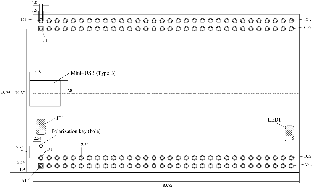
The following drawing shows the measurements and the location of the of the described elements.
Click on the image for a larger version or download the PDF version.
JP1
Jumper JP1 specifies the I2C address of the EEPROM:
| JP1 | I2C address |
| open | 0xA2 |
| close | 0xAA |
The EZ-USB FX2 Microcontroller searches for the firmware at the address 0xA2 which is the default address (jumper open).
The main purpose of this jumper is to disable the EEPROM boot-load. If, for example, the EEPROM was programmed with a corrupt firmware the Microcontroller can be booted with the internal default firmware by short cutting the two pads of jumper JP1 during powering-on the USB-FPGA-Module.
LED1
LED1 indicates the configuration state of the FPGA as follows:
| LED1 | FPGA |
| on | unconfigured |
| off | configured |
I/O Connector
Two 2x32 pin, 2.54mm pitch connectors delivers the I/O signals and are used for the power supply. The drawing shows the position of the connectors.
The I/O connector of the USB-FPGA-Module 1.2 is mechanical upward compatible to the I/O Connector of the Spartan 6 USB-FPGA-Module 1.11.
The following Pinlist can also be downloaded in Gnumeric or Excel format. These files contains the data for all ZTEX USB-FPGA-Modules and also include a list of connections (several sheets).
| Pinlist | ||||||
| A | B | C | D | |||
| 1 | 5..15V | 5..15V | USB_5V | USB_5V | 1 | |
| 2 | GND | GND | 5V (unused) | 5V (unused) | 2 | |
| 3 | INT4 | T0 | CLKOUT | 5V (unused) | 3 | |
| 4 | T1 | T2 | GND | GND | 4 | |
| 5 | BKPT | GND | INT5# | WAKEUP* | 5 | |
| 6 | SCL | SDA | 3.3V | 3.3V | 6 | |
| 7 | 3.3V | 3.3V | VCCO_TOP | VCCO_TOP | 7 | |
| 8 | TxD0 | RxD0 | GND | 5~L20P_7 | 8 | |
| 9 | TxD1 | RxD1 | PE7 | 4~IO/VREF_7 | 9 | |
| 10 | 2.5V | 2.5V | PE6 | 2~IO_L01N_7/VRP_7 | 10 | |
| 11 | 1.2V | 1.2V | PE5 | 1~IO_L01P_7/VRN_7 | 11 | |
| 12 | 74~IO_L01N_3/VRP_3 | 73~IO_L01P_3/VRN_3 | PE4 | 141~IO_L01N_0/VRP_0 | 12 | |
| 13 | 76~IO | GND | PE3 | 140~IO_L01P_0/VRN_0 | 13 | |
| 14 | 78~IO_L20N_3 | 77~IO_L20P_3 | PE2 | 137~IO_L27N_0 | 14 | |
| 15 | 80~IO_L21N_3 | 79~IO_L21P_3 | PE1 | 135~IO_L27P_0 | 15 | |
| 16 | 3.3V | 3.3V | PE0 | 132~IO_L30N_0 | 16 | |
| 17 | 83~IO_L22N_3 | 82~IO_L22P_3 | GND | 131~IO_L30P_0 | 17 | |
| 18 | 85~IO_L23N_3 | 84~IO_L23P_3/VREF_3 | 2.5V | 2.5V | 18 | |
| 19 | 87~IO_L24N_3 | 86~IO_L24P_3 | 1.2V | 130~IO_L31N_0 | 19 | |
| 20 | 90~IO_L40N_3/VREF_3 | 89~IO_L40P_3 | 128~IO_L32N_0/GCLK7 | 129~IO_L31P_0/VREF_0 | 20 | |
| 21 | GND | GND | 125~IO_L32N_1/GCLK5 | 127~IO_L32P_0/GCKL6 | 21 | |
| 22 | VCCO_RIGHT | VCCO_RIGHT | 123~IO_L31N_1/VREF_1 | 124~IO_L32P_1/GCLK4 | 22 | |
| 23 | 1.2V | 1.2V | 119~IO_L28N_1 | 122~IO_L31P_1 | 23 | |
| 24 | 93~IO_L40N_2 | 92~IO_L40P_2/VREF_2 | 116~IO | 118~IO_L28P_1 | 24 | |
| 25 | 96~IO_L24N_2 | 95~IO_L24P_2 | 112~IO_L01P_1/VRN_1 | 113~IO_L01N_1/VRP_1 | 25 | |
| 26 | 98~IO_L23N_2/VREF_2 | 97~IO_L23P_2 | GND | GND | 26 | |
| 27 | 100~IO_L22N_2 | 99~IO_L22P_2 | VCCO_TOP | VCCO_TOP | 27 | |
| 28 | 103~IO_L21N_2 | 102~IO_L21P_2 | 1.2V | 1.2V | 28 | |
| 29 | 105~IO_L20N_2 | 104~IO_L20P_2 | 2.5V | TDI | 29 | |
| 30 | 108~IO_L01N_2/VRP_2 | 107~IO_L01P_2/VRP_2 | M0 | TMS | 30 | |
| 31 | VCCO_RIGHT | VCCO_RIGHT | M1 | TCK | 31 | |
| 32 | GND | GND | GND | TDO | 32 | |
| Summary | ||||
| A/B | C/D | |||
| FPGA-IO | 29 | FPGA-IO | 23 | |
| Serial | 4 | FX2-IO | 8 | |
| I2C | 2 | CLK | 1 | |
| Timer | 3 | Interrupt | 1 | |
| Interrupt | 1 | Wakeup | 1 | |
| Breakpoint | 1 | JTAG | 6 | |
| 3.3V | 4 | 3.3V | 2 | |
| VCCO_RIGHT | 4 | VCCO_TOP | 4 | |
| 2.5V | 2 | 2.5V | 3 | |
| 1.2V | 4 | 1.2V | 3 | |
| 5..15V | 2 | 5V | 3 | |
| GND | 8 | USB 5V | 2 | |
| GND | 7 | |||
| FPGA-GPIO | 29 | FPGA-GPIO | 23 | |
| SIO (special I/O) | 11 | FX2-GPIO | 8 | |
| Power | 24 | SIO (special I/O) | 9 | |
| Sum | 64 | Power | 24 | |
| Sum | 64 | |||
References
- Product Homepage
- Eagle Library of the I/O connector
- Pinlist and the List of Connections in Gnumeric and Excel format